SEM Imaging of Biological Samples
Przegląd
Source: Peiman Shahbeigi-Roodposhti and Sina Shahbazmohamadi, Biomedical Engineering Department, University of Connecticut, Storrs, Connecticut
A scanning electron microscope (SEM) is an instrument that uses an electron beam to nondestructively image and characterize conductive materials in a vacuum. As an analogy, an electron beam is to the SEM as light is to the optical microscope. The difference is that the electron microscope yields images of much higher resolution and magnification. The best optical microscopes typically have a resolution down to 200 nm, whereas SEMs usually claim a resolution of 0.5 nm. This is due to the fact that optical microscopes are limited by the diffraction of waves, a function of the wavelength, which is around 500 nm for visible light. Conversely, the SEM uses an energized electron beam, which as a wavelength of 1 nm. This characteristic makes them very dependable tools for the study of nano and microstructures. Electron microscopes also enable the study of biological samples with feature sizes too small for optical microscopy.
This demonstration provides an introduction to sample preparation and initial image acquisition of biological samples using a scanning electron microscope. In this case, a collagen-hydroxyapatite (HA) cellular scaffold will be studied. The vacuum environment of the SEM and the induced charging by the electron beam on non-conductive samples (such as organic matter) creates challenges that will be addressed in the preparation. The advantages and disadvantages of different imaging methods as they relate to resolution, depth of focus and sample type will also be discussed. The purpose of this demonstration is to give the participant more information on SEM to determine if this microscopy module is the best fit for a type of biological sample.
Zasady
When a high-energy electron beam (typically ranging from 5-30 keV) hits a sample, a range of signals are emitted from the sample. These interactions can be used to study topography, crystallography, electrical potential and local magnetic fields. The electrons undergo two types of scattering: elastic and inelastic. Inelastic scattering causes the emission of secondary electrons. These low energy electrons (~50 eV) are the outer shell electrons of the sample atoms that acquire just enough energy to leave the surface of the atom. The scattering of secondary electrons provides topographical information, as the energy level of the electrons leaving the sample atom is not high enough to travel through the sample. Therefore only surface level information is collected by the detector.
Elastic scattering, on the other hand, is not caused by dislodged electrons from the sample atoms. It is the principal beam of electrons after interaction with the nucleus, as seen in Figure 1. These electrons do not change their energy or speed, but they do change their direction based on their interaction with the nucleus. The detection of these electrons provides compositional information, and their varying contrast upon interaction with atoms of different atomic weights allows the user to distinguish differences in sample composition. In biological samples, this can be used to study embedded or attached nanoparticles and nanostructures with heavier atomic weights, such as gold or iron.
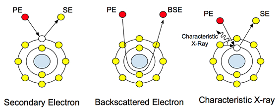
Figure 1: Atomic interactions with the principal electrons (PE) and how they create the different signals.
Sample preparation is an important procedure, especially for biological samples. In order to obtain high-resolution SEM images, electrons need to reach the sample. Then, the signals that are the result of the interaction between the electrons and the sample need to reach the detectors. This means that the instrument must work under a high vacuum to prevent electron scattering before the beam reaches the sample and the signals reach the detectors. This vacuum is highly sensitive and can pull particulate matter off of the sample, meaning it is important to make sure the sample is dry and free of particulates.
Another consideration in sample preparation is the nature of the electron beam. Because the beam is composed of highly charged particles, When a non-conductive sample is bombarded with highly charged particles from the electron beam, there is a buildup of charges on the surface that affect the deflection of the electron beam and cause a large increase in beam scatter. By coating the sample with a conductive layer before imaging, these charging artifacts in the image can be avoided.
The methods described here are applicable to most non-conductive materials. A coating is necessary to mitigate charging artifacts. The collagen-HA cellular scaffold was made by the following synthesis steps: co-precipitation of collagen with HA into the composite gel, slurry creation and freeze casting, crosslinking the scaffold and final drying. This final drying is completed over 5 days in a vacuum dryer and sufficiently dries the sample for SEM analysis without affecting the structural properties of the scaffolds. However, when imaging cells, the main concern when preparing the sample is preserving the cell structure. Chemical and resin-based fixation methods are commonly used to observe cells while preserving the structure of cells, such as glutaraldehyde fixation and epoxy and acrylic resins. Typically, glutaraldehyde is used as a fixative that creates crosslinkages in the cytoplasm of cells but also causes a drop in the pH. Therefore, buffering is needed when preparing samples with glutaraldehyde. The addition of these techniques allows the structure of the cell to most resemble its structure when it was alive [3].

Figure 2: Gold-palladium sputter coater showing the sample chamber (silver vessel on top) and vacuum (left) and current (right) gauges. In this model, a current of 2 mA is used with a chamber vacuum of 0.1 torr, which is kept constant using an argon leak valve.
Procedura
1. Sample Preparation
- Wear gloves and take precautions to avoid contamination when handling the sample.
- Make sure that the sample on the slide is dried and there is no contamination on the sample. This is because SEM measures surface characterization, and these defects can severely hinder the signal.
- If the sample is loaded on a standard glass slide, decrease the size of the sample by scoring the slide with a diamond tipped glass cutter in a straight line and gently push on the scored line away from the body until the glass fractures.
- Depending on the sample, choose a coating that does not have the same elemental composition (it would hinder the signal received by EDS). For this demonstration, a gold-palladium coating is used.
- Use the sputter coater as directed. Let the machine sputter the sample for around 40 s for a thin coating with adequate coverage.
- Mount the sample onto an SEM stub using conductive double-sided carbon tape. This tape should also be placed from the stage to the top of the slide that was sputtered to ground the sample if it is mounted on a non-conductive slide. A thin layer of conductive silver paint could also be used to increase the conductivity of the sample to the stage.
- Mount the stub onto the stage and tighten the screw on the side.
2. Imaging Procedure
- Load the stage into the chamber. Shut and seal the door. Then hit the "Transfer" button to open the passage from the loading chamber to the vacuum.
- Once the transfer button stops blinking and the internal door is open, the sample can be moved into the vacuum chamber by screwing in the metal rods and pushing the sample into the chamber.
- Unscrew the rod, retract and secure the rod fully into the load chamber, and press "store" to close off the load chamber from the vacuum chamber. The sample is now loaded and the rest of the process takes place from the computer workstation.
- Move the stage using the controller and by opening the stage navigation panel until it is in your field of view.
- Move the sample vertically until the working distance is 5-10 mm. When moving the stage in the z-direction, turn on the chamber camera to ensure your sample does not get to close to the electron gun.
- Turn the extra high tension (EHT) beam on. Note that you may also need to open the column if it has been off for a while.
- Select the SE2 signal from the detector options.
- Use a kV setting of about 5 kV for initial imaging, and then increase to 20-30 kV for more signal using the back-scatter mode. If the sample wasn't coated, keep the keV low to prevent too many charging artifacts in the image and to prevent sample damage.
- If there is no clear image, turn the focus, brightness, and contrast knobs until a structure is visible. This will be a reference for refinement.
- Turn the focus knob on coarse mode until an image is visible. Then switch to fine to find the best focus.
- Use stage navigation (not in the z-direction) and the magnification to find an area to save an image from.
- Decrease the scan speed and turn on line averaging to acquire a better image for saving.
- Save the image by right clicking and saving to a file location.
- Insert the BSD and move the stage back to a z-position where the sample is focused.
- Repeat steps 8-11 while looking for areas of contrast that indicate a higher atomic number.
- Remove the BSD when done.
- When ready to remove the sample, hit the button "exchange".
- Move the sample back into the load chamber and hit "store" then "vent".
Wyniki
The SEM images in Figures 3 and 4 show that the imaged structure is highly three dimensional with microscale features. Image quality is affected by the focus and the thickness of the sputter coating.

Figure 3: The following images demonstrate how the sample focus can affect image quality. In the image on the right, the whole field of view is in focus, whereas it is out of focus on the left. Playing with parameters like the focus can provide a much better image.

Figure 4: Images of collagen-hydroxyapatite sample.
Wniosek i Podsumowanie
Here we demonstrated the depth of focus, field of view and maximum resolution and magnification of an electron microscope and how these properties can be used to view biological samples. This demonstration was designed to help viewers decide which microscopy module is the best for a certain application. As demonstrated, SEM has a very high depth of focus, much higher resolution and greater magnifications. However, it is not appropriate for all sample types.
This demonstration introduced the principles of electron microscopy and showed several of their applications in research labs. Electron microscopes are used for inspection, characterization and quality control. For example, they are used to visualize ICs, circuit boards, crack propagation and nano-electromechanical systems. In the field of biology these instruments play a key role as well. There are even electron microscopes especially designed to accommodate wet biological samples. These biological samples range from tissues to bone, cells and microorganisms. Using additional detectors can enable even more analysis, such as precise surface analysis.
Materials List
| Name | Company | Catalog Number | Comments |
| Equipment | |||
| Biosample | |||
| Carbon or Gold coater | |||
| Cross beam-SEM | ZEISS | ||
| Collagen-Hydroxyappetite Cellular Scaffolds | Developed by Wei Laboratory at University of Connecticut |
Odniesienia
- Oatley, C. W., W. C. Nixon, and R. F. W. Pease. "Scanning electron microscopy." Advances in Electronics and Electron Physics 21 (1966): 181-247.
- Goldstein, Joseph, et al. Scanning electron microscopy and X-ray microanalysis: a text for biologists, materials scientists, and geologists. Springer Science & Business Media, 2012.
- Carol Heckman, et al. Preparation of cultural cells for scanning electron microscope. Nature Protocols Network, 2007, doi:10.1038/nprot.2007.504
Tagi
Przejdź do...
Filmy z tej kolekcji:

Now Playing
SEM Imaging of Biological Samples
Biomedical Engineering
23.5K Wyświetleń

Imaging Biological Samples with Optical and Confocal Microscopy
Biomedical Engineering
35.7K Wyświetleń

Biodistribution of Nano-drug Carriers: Applications of SEM
Biomedical Engineering
9.3K Wyświetleń

High-frequency Ultrasound Imaging of the Abdominal Aorta
Biomedical Engineering
14.4K Wyświetleń

Quantitative Strain Mapping of an Abdominal Aortic Aneurysm
Biomedical Engineering
4.6K Wyświetleń

Photoacoustic Tomography to Image Blood and Lipids in the Infrarenal Aorta
Biomedical Engineering
5.7K Wyświetleń

Cardiac Magnetic Resonance Imaging
Biomedical Engineering
14.7K Wyświetleń

Computational Fluid Dynamics Simulations of Blood Flow in a Cerebral Aneurysm
Biomedical Engineering
11.7K Wyświetleń

Near-infrared Fluorescence Imaging of Abdominal Aortic Aneurysms
Biomedical Engineering
8.2K Wyświetleń

Noninvasive Blood Pressure Measurement Techniques
Biomedical Engineering
11.9K Wyświetleń

Acquisition and Analysis of an ECG (electrocardiography) Signal
Biomedical Engineering
104.8K Wyświetleń

Tensile Strength of Resorbable Biomaterials
Biomedical Engineering
7.5K Wyświetleń

Micro-CT Imaging of a Mouse Spinal Cord
Biomedical Engineering
8.0K Wyświetleń

Visualization of Knee Joint Degeneration after Non-invasive ACL Injury in Rats
Biomedical Engineering
8.2K Wyświetleń

Combined SPECT and CT Imaging to Visualize Cardiac Functionality
Biomedical Engineering
11.0K Wyświetleń
Copyright © 2025 MyJoVE Corporation. Wszelkie prawa zastrzeżone