
Scanning Electron Microscopy (SEM)
Overview
Source: Laboratory of Dr. Andrew J. Steckl — University of Cincinnati
A scanning electron microscope, or SEM, is a powerful microscope that uses electrons to form an image. It allows for imaging of conductive samples at magnifications that cannot be achieved using traditional microscopes. Modern light microscopes can achieve a magnification of ~1,000X, while typical SEM can reach magnifications of more than 30,000X. Because the SEM doesn’t use light to create images, the resulting pictures it forms are in black and white.
Conductive samples are loaded onto the SEM’s sample stage. Once the sample chamber reaches vacuum, the user will proceed to align the electron gun in the system to the proper location. The electron gun shoots out a beam of high-energy electrons, which travel through a combination of lenses and apertures and eventually hit the sample. As the electron gun continues to shoot electrons at a precise position on the sample, secondary electrons will bounce off of the sample. These secondary electrons are identified by the detector. The signal found from the secondary electrons is amplified and sent to the monitor, creating a 3D image. This video will demonstrate SEM sample preparation, operation, and imaging capabilities.
Principles
Electrons are generated by heating by the electron gun, which acts like a cathode. These electrons are propelled towards the anode, in the same direction as the sample, due to a strong electric field. After the beam of electrons is condensed, it enters the objective lens, which is calibrated by the user to a fixed position on the sample. (Figure 1)
Once the electrons strike the conductive sample, two things can happen. First, the primary electrons that hit the sample will tunnel through it to a depth which is dependent on the energy level of those electrons. Then, the secondary and backscattered electrons will hit the sample and reflect outwards from it. These reflected electrons are then measured either by the secondary electron (SE) or backscattered (BS) detector. After signal processing takes place, an image of the sample is formed on the screen.1
In SE mode, secondary electrons are attracted by positive bias on the front of detector because of their low energy. The signal intensity is varied depending on the angle of the sample. Therefore, SE mode provides highly topographical images. On the other hand, in BS mode, the direction of electrons is almost directly opposite of the e-beam direction and the detection intensity is proportional to the atomic number of the sample. Therefore, it is less topographical, but useful for compositional images. BS mode is also less affected by the charging effect on the sample, which is beneficial for non-conductive samples.1
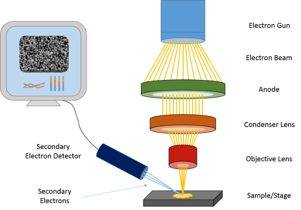
Figure 1. Schematic of the SEM.
Procedure
1. Preparation of the Sample
- Place sample onto sample stub. If necessary, carbon tape may be used to adhesively bond the sample to the stub.
- Place the sample into a gold sputtering system. Using a mini-gold sputter, sputter gold for 30 s at ~ 70 mTorr pressure. A different gold layer thickness may be necessary depending on the geometry of the sample. More rough or porous surface requires a longer sputtering time.
- Remove stub from gold sputtering system.
2. Sample Insertion and SEM Startup
- Vent the SEM chamber, allowing the chamber to reach nominal pressure.
- Open the SEM sample compartment and take out the sample stage.
- Insert the sample stub containing the sample onto the stage. Tighten the stub into place.
- If the z-distance cannot be controlled by software, make sure the sample stage with sample stub has proper height to obtain the better image.
- Put the sample stage into sample chamber. Close the sample compartment.
- Turn on the pumps and allow system to reach vacuum. The system will notify the user when this is completed.
- Open the SEM software. Select desired operating voltage ranging from 1–30 kV. Higher operating voltage gives better image contrast, but can yield lower resolution if charges accumulate in the sample.
3. Capturing the SEM Image
- Begin ‘Auto Focus’ in the SEM software by clicking on the key icon. This will acquire a focused image of the sample to use as a starting point.
- Make sure the magnification is set to the minimum zoom level of 50X.
- Select ‘fast scan’ mode.
- Adjust the focus in coarse mode until a rough focus is acquired.
- Adjust the stage manually using the exterior knobs so that the region of interest is visible on the display.
- Increase the magnification level until the desired feature is observed. Adjust the coarse focusing knob to roughly focus the image at this magnification. Then, improve the focus using the fine focusing knob to get a focused image at the desired magnification level. This step will be repeated whenever the magnification level is increased.
- Once the desired magnification is reached, adjust the fine focusing knob to improve clarity.
- To optimize image clarity, increase the magnification close to the maximum level, and then focus the image using the fine focus knob. If a clear image cannot be obtained, adjust the stigmation in both the x and y direction. Keep adjusting the focus and stigmations until the clearest image is obtained at the exaggerated magnification level.
- After reaching a quality image of the sample, go back to the desired magnification level. The image can be taken by pressing the photo button in either ‘slow photo’ or ‘fast photo’ mode. The ‘slow photo’ mode gives better quality and high resolution of the image.
4. Making Measurements Using the SEM Software
- In the ‘Panels’ dropdown list, select ‘M. Tools’.
- Various measurements such as length, area, and angle can be measured directly in the SEM software. To perform one of these measurements, click on the desired icon in the M. Tools window.
- Scroll to the measurement site on the SEM image. Measurements are done by clicking on the image to create points of reference that will be analyzed by the software. Data points measured can be inserted directly onto the image if desired by the user.
- Images are then saved to the computer.
Results
The SEM, seen in Figure 2a, has been used for making measurements and acquiring sample photos. The sample consisted of sodium chloride (NaCl) salt. It was placed onto the stub as seen in Figure 2b, then a few nanometers of gold was sputtered onto it to make it conductive. The conductive sample was then placed into the SEM sample area as seen in Figure 2c.
SEM images were obtained at 50X, 200X, 500X, 1,000X, and 5,000X magnification levels as seen in Figure 3. Figure 3a shows a birds-eye view of the salt sample at 50X magnification. Figure 3b then zooms in to an individual salt particle at a magnification of 200X. Figure 3c shows this same magnification level but includes area and diameter measurements made within the SEM software. Figure 3d then zooms to 500X, showing the area of interest on the salt particle. Figure 3e shows a magnification of 1,000X, allowing one to observe the corner of the salt particle that has been damaged. Figure 3f shows a magnification of 5,000X, allowing the user to view the structure of the salt particle.

Figure 2. (a) Image of SEM. (b) NaCl salt placed onto sample stub with carbon tape. (c) Sample stub placed into SEM sample stage after it was treated with gold coating.

Figure 3. SEM images of sample at various magnification levels: (a) 50X, (b) 200X, (c) 200X with measurements, (d) 500X, (e) 1,000X, and (f) 5,000X.
Application and Summary
The SEM is a very powerful tool that is common in most research institutions because of its ability to image any object that is conductive, or has been treated with a conductive coating. The SEM has been used to image objects such as semiconductor devices,2 biological membranes,3 and insects,4 among others. We have also used the SEM to analyze nanofibers and paper-based materials, biomaterials, micropatterned structures. Of course, there are materials, such as liquids, that can’t be placed into a standard SEM for imaging, but continuous development of Environmental Scanning Electron Microscopes (ESEM) allows for such functionality. ESEM is similar to SEM in that it uses an electron gun and analyzes the electron interaction with the sample. The main difference is that the ESEM is split into two separate chambers. The top chamber consists of the electron gun and goes into a high vacuum state, while the lower chamber contains the sample and enters a high pressure state. Because the sample area does not need to enter a vacuum, wet or biological samples can be used during the imaging process. Another ESEM benefit is that the sample does not need to be coated with a conductive material. However, ESEM has some disadvantages of low image contrast and small working distance due to gaseous environment in the sample chamber. . The general rule of thumb is that if you are able to coat a sample with a conductive layer, then it can be imaged in an SEM, allowing for almost all solid objects to be analyzed.
References
- Goldstein, J., Newbury, D., Joy, D., Lyman, C., Echlin, P., Lifshin, E., Sawyer, L., Michael, J. Scanning Electron Microscopy and X-ray Microanalysis. 3rd Ed. Springer, New York, NY. (2003).
- Purandare, S., Gomez, E.F., Steckl, A.J. High brightness phosphorescent organic light emitting diodes on transparent and flexible cellulose films. Nanotechnology. 25, 094012 (2014).
- Masuda, Y., Yamanaka, N., Ishikawa, A., Kataoka, M., Aral, T., Wakamatsu, K., Kuwahara, N., Nagahama, K., Ichikawa, K., Shimizu, A. Glomerular basement membrane injuries in IgA nephropathy evaluated by double immunostaining for a5(IV) and a2(IV) chains of type IV collagen and low-vacuum scanning electron microscopy. Clinical and Experimental Nephrology. 1-9. (2014).
- Kang, J.H., Lee, Y.J., Oh, B.K., Lee, S.K. Hyun, B.R. Lee, B.W, Choi, Y.G., Nam, K.S., Lim, J.D. Microstructure of the water spider (Argyroneta aquatic) using the scanning electron microscope Journal of Asia-Pacific Biodiversity. 7 484-488 (2014).
Disclosures
Tags
Skip to...
Videos from this collection:

Now Playing
Scanning Electron Microscopy (SEM)
Analytical Chemistry
87.2K Views

Sample Preparation for Analytical Characterization
Analytical Chemistry
84.8K Views

Internal Standards
Analytical Chemistry
204.9K Views

Method of Standard Addition
Analytical Chemistry
320.2K Views

Calibration Curves
Analytical Chemistry
797.1K Views

Ultraviolet-Visible (UV-Vis) Spectroscopy
Analytical Chemistry
623.8K Views

Raman Spectroscopy for Chemical Analysis
Analytical Chemistry
51.2K Views

X-ray Fluorescence (XRF)
Analytical Chemistry
25.4K Views

Gas Chromatography (GC) with Flame-Ionization Detection
Analytical Chemistry
282.1K Views

High-Performance Liquid Chromatography (HPLC)
Analytical Chemistry
384.8K Views

Ion-Exchange Chromatography
Analytical Chemistry
264.6K Views

Capillary Electrophoresis (CE)
Analytical Chemistry
94.0K Views

Introduction to Mass Spectrometry
Analytical Chemistry
112.3K Views

Electrochemical Measurements of Supported Catalysts Using a Potentiostat/Galvanostat
Analytical Chemistry
51.4K Views

Cyclic Voltammetry (CV)
Analytical Chemistry
125.3K Views
Copyright © 2025 MyJoVE Corporation. All rights reserved