
Focused Ion Beams
Обзор
Source: Sina Shahbazmohamadi and Peiman Shahbeigi-Roodposhti-Roodposhti, School of Engineering, University of Connecticut, Storrs, CT
As electron microscopes become more complex and widely used in research labs, it becomes more of a necessity to introduce their capabilities. Focused ion beam (FIB) is an instrument that can be employed in order to fabricate, trim, analyze and characterize materials on mico- and nano-scales in a wide variety of fields from nano-electronics to medicine. FIB systems can be thought of as a beam of ions that can be used to mill (sputter), deposit, and image materials on micro- and nano-scales. The ion columns of FIBs are commonly integrated with the electron columns of scanning electron microscopes (SEMs).
The goal of this experiment is to introduce the state of the art in focused ion beam technologies and to show how these instruments can be used in order to fabricate structures that are as small as the smallest membranes that are found in the human body.
Принципы
FIB systems use a beam of ions to mill, deposit and image micro- and nano-scale samples. The beam is formed in a high-vacuum environment where selective electric potentials are used to ionize and extract gallium from a liquid metal ion source (LMIS). This beam can be directed and focused with electromagnetic lenses similar to light in a traditional, optical microscope. The beam then rasters to cover an area on the sample. With a different kind of source, an electron beam can be used for nondestructive imaging and characterization without sputtering the sample surface, much like scanning electron microscopy (SEM). The combination of SEM and FIB paves a path for very innovative ion beam millings and characterization. Additionally, three-dimensional information can be obtained by combining the electron and ion beam operations to perform a tomography (i.e. mill a slice with ion beam, image with electron beam, and repeat). Generally, conductive samples are ideal for FIB and SEM because they do not collect charge and thereby affect the pathway to imaging, milling, and deposition. However, non-conductive samples like most polymers and biological samples can be probed with the use of charge correction, conductive coating, variable pressure settings, and low energy beam settings. Having an understanding of the basics of ion beam-solid interactions may improve the ability to achieve optimal results using an FIB system. The mechanics of ion beam-solid interactions consists in the following events: primary ions of the focused beam bombard the surface, sputter material, eject secondary electrons and implant themselves.
Milling occurs due to the physical sputtering of the target. In order to understand the sputtering process, the interactions between the ion beam and the target must be explored. Sputtering takes place as a consequence of a series of elastic collisions in which momentum is transferred from the incident ions to the target atoms within a region that is called cascade region. This process is similar to what happens when a cue ball hits the object balls when the break shot is taken. An atom on the surface of the target may be sputtered if it receives a kinetic energy that exceeds its surface binding energy (SBE). The surface binding energy is the energy required to remove a surface atom from its bulk lattice. A portion of these ejected atoms might be ionized. Because of ion bombardment, inelastic interactions can also happen. These interactions produce phonons, plasmons in metals, and secondary electrons (SE). A standard FIB employs secondary electrons in order to produce an image. Deposition can also be accomplished by deploying small amounts of precursor gas molecules to the surface of the material and using the impinging ions to facilitate a chemical reaction where the material is deposited onto the surface. Though, for this study, milling and imaging are the only mechanisms covered.
Процедура
1. Fabrication of a perforated filter from a 300nm thick silicon oxide membrane comparable in scale to the kidneys' endothelial cytoplasm
- Load the as-prepared membrane into the FIB chamber. The membranes are often prepared by professionals (when creating Wheatstone bridges) and can be acquired at semiconductor fabrication sites. To prepare one yourself, photolithography must be used. The details of this process can be seen in the photolithography video of the "Bioengineering Collection" on the JoVE website. NOTE: Be certain to wear nitrile gloves when handling the sample or when coming in contact with any internal components of the FIB/SEM. The environment must be kept very clean and free of any skin oils.
- Turn the focused ion beam and electron gun on and adjust the sample to achieve the coincident-eucentric point. This is the point where the area of interest (the membrane) is in the line of electrons and ions for tilt angles ranging from 0-54 degrees.
- Adjust the ion beam current and accelerating voltage of the FIB to 30kV and 100pA and focus on an area close to the area to be milled. Draw a matrix of circles through the FIB milling program of a diameter around 50nm with a center to center distance of 150nm (see Figure 1).
- Change to electron beam and image the area at an accelerating voltage of 5kV.

Figure 1: FIB milled holes in silicon oxide membrane creating particle filter.
2. Milling a logo on a hair
- Put a hair strand on a microscope stub using carbon tape
- Gold/Carbon coat the hair strand using a sputter coater. This tool coats the sample in a few nanometers of a conductive material so it can be imaged/sputtered with minimal charging artifacts.
- Turn the focused ion beam and electron gun on and adjust for the coincident-eucentric point.
- Adjust the ion beam current and accelerating voltage to 30kV with a 100pA aperture, respectively, and focus on an area of about 15um x 15um close to the area to be milled.
- Load the pattern/logo to be milled as a bitmap and adjust the beam current and accelerating voltage and start the milling.
- Change to electron beam and image the area. This is shown in Figure 2.
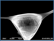
Figure 2: "Happy Holidays" milled on a spider web with FIB.
Заявка и Краткое содержание
This experiment demonstrated how using electron microscopes and focused ion beams enable researchers to manipulate and fabricate microscale structures. The molecular nature of the focused ion beam-material interaction provides FIB with a unique ability to manipulate materials on the micro- and nano-scales. By carefully considering how the beam interacts with the material, mitigating charging artifacts and setting the system for optimal milling quality, a researcher can produce unique patterns on biological and non-biological materials that can, in the case of silicon oxide membrane, perform just like its anatomical counterpart. FIBs show a lot of potential in this area of research but techniques and the materials used should improve a lot more for finding their way into the living organisms. These instruments and techniques alongside tissue engineering techniques can revolutionize the way we approach treatment of the organs in the near future.
This experiment focused on giving an introduction to focused ion beam (FIB) systems and demonstrating what they can do. Their applications are vast. The exercises here highlighted some applications in biology, which can range from micron size cross sectioning to the examination of bone and tissue to three-dimensional reconstruction of small parts of an organ. It is important to note that FIB is not just a tool for tissue engineering. It has much history with microelectronics, geological studies, additive manufacturing, spray coatings, transmission electron microscopy (TEM) sample preparation and general material characterization. Examples within these topics are widespread and can be found in any FIB-related literature.
Перейти к...
Видео из этой коллекции:

Now Playing
Focused Ion Beams
Materials Engineering
9.0K Просмотры

Optical Materialography Part 1: Sample Preparation
Materials Engineering
15.6K Просмотры

Optical Materialography Part 2: Image Analysis
Materials Engineering
11.2K Просмотры

X-ray Photoelectron Spectroscopy
Materials Engineering
21.9K Просмотры

X-ray Diffraction
Materials Engineering
89.7K Просмотры

Directional Solidification and Phase Stabilization
Materials Engineering
6.7K Просмотры

Differential Scanning Calorimetry
Materials Engineering
38.7K Просмотры

Thermal Diffusivity and the Laser Flash Method
Materials Engineering
13.4K Просмотры

Electroplating of Thin Films
Materials Engineering
20.2K Просмотры

Analysis of Thermal Expansion via Dilatometry
Materials Engineering
16.0K Просмотры

Electrochemical Impedance Spectroscopy
Materials Engineering
23.4K Просмотры

Ceramic-matrix Composite Materials and Their Bending Properties
Materials Engineering
8.4K Просмотры

Nanocrystalline Alloys and Nano-grain Size Stability
Materials Engineering
5.2K Просмотры

Hydrogel Synthesis
Materials Engineering
23.8K Просмотры
Авторские права © 2025 MyJoVE Corporation. Все права защищены