Flyback Converter
Genel Bakış
Source: Ali Bazzi, Department of Electrical Engineering, University of Connecticut, Storrs, CT.
A flyback converter is a buck-boost converter, which can both buck and boost. It has electrical isolation between the input and the output using a coupled inductor or a "flyback transformer." This coupled inductor enables a turns ratio that provides both voltage step-up and step-down capability, like in a regular transformer but with energy storage using the air-gap of the coupled inductor.
The objective of this experiment is to study different characteristics of a flyback converter. This converter operates like a buck-boost converter but has electrical isolation through a coupled inductor. Open-loop operation with a manually-set duty ratio will be used. An approximation of the input-output relationship will be observed.
İlkeler
To better understand the flyback converter, first, one must understand a buck-boost converter. The flyback converter circuit can then be derived from the buck-boost converter.
The buck-boost converter, as its name implies, can either step-up or step-down a DC voltage input to higher or lower voltage, respectively. To derive a buck-boost converter circuit, a buck and boost converter are cascaded as shown in Fig. 1 (a). A current source/sink is used as the load for the buck converter and input to the boost converter, causing the boost converter to be flipped to maintain the input voltage polarity. Buck-boost converters thus have a reversed output voltage polarity.
As can be seen in Fig. 1 (b), the current source/sink can be replaced with a large inductor that acts as a current source or sink. However, "C1" is no longer needed, as the intermediate voltage across "L3" does not have to have a very small ripple voltage. Also Switch 2 is no longer needed since it may cause a short-circuit across "L2" and "L3." The circuit is thus updated as shown in Fig. 1 (c).
Also, Diode 1 was used in the buck converter to provide a current path for the inductor "L1," but "L1" and "L2" can be removed since a smooth current is no longer needed in the intermediate stage. Diode 1 can thus also be removed, as shown in Fig. 1 (d) and (e). The bottom-side Diode 2 can be moved to the top side or left on the bottom side, as shown in Fig. 1 (e) which is the most common buck-boost converter circuit implementation.
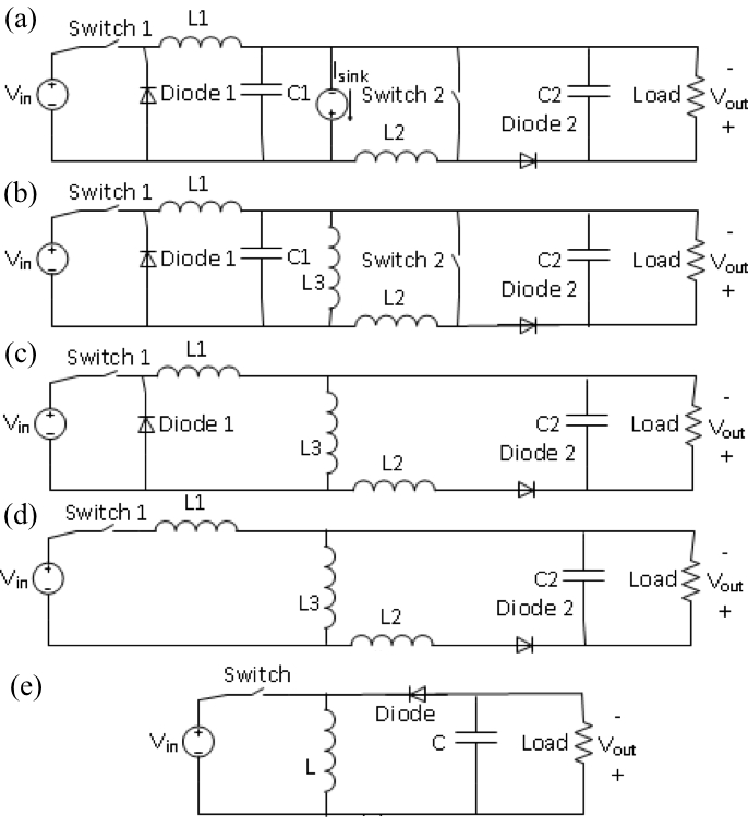
Figure 1. Derivation of a buck-boost converter circuit from cascaded buck and boost converters
The flyback converter goes one step further than the buck-boost converter by providing electrical isolation between the input and output voltages. This is desired in many power supply applications where grounds on the source and load sides need to be separated. Typically, flyback converters are used in ratings up to 200 W. The schematic shown in Fig. 2 illustrates how a flyback converter is derived from a buck-boost converter.
When the switch is on in a buck-boost converter, the diode is reverse biased and energy is stored in the inductor. When the switch is off, the inductor can either absorb energy from the capacitor once the diode is on, or can supply the capacitor and load with energy. This provides the step-down and step-up flexibility. However, the inductor can be replaced with a coupled inductor or flyback transformer to provide electrical isolation with the output side as shown in Fig. 2 (b). The switch being on the top side requires a high-side gate driver circuit, which is more elaborate and requires more components than a low-side circuit. Therefore, the switch can simply be moved such that one of its terminals is grounded and thus it requires a simple low-side gate driver as shown in Fig. 2 (c). In order to have the input and output voltage polarities on the same side, the output diode is reversed along with the transformer's polarity. The final flyback converter is shown in Fig. 2 (d).
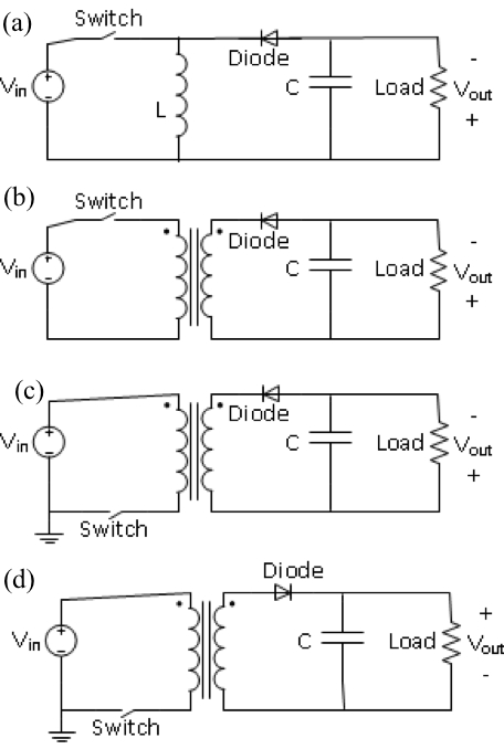
Figure 2. Derivation of a flyback converter circuit from a buck-boost converter circuit
Prosedür
ATTENTION: This experiment is designed to limit the output voltage to be less than 50V DC. Only use duty ratios, frequencies, input voltage, or loads that are given here.
This experiment will utilize the DC-DC converter board provided by HiRel Systems. http://www.hirelsystems.com/shop/Power-Pole-Board.html
Information about the board operation can be found in this collections video “Introduction to the HiRel Board.”
The procedure shown here applies to any simple flyback converter circuit that can be built on proto boards, bread boards, or printed circuit boards.
1. Board setup:
- Connect the ±12 signal supply at the "DIN" connector but keep "S90" OFF.
- Make sure that the PWM control selector is in the open-loop position.
- Set the DC power supply at 16 V. Keep its output disconnected from the board for now.
- Before connecting the load resistor, adjust it to 10 Ω.
- Build the circuit shown in Fig. 3 by using the lower MOSFET and flyback magnetic board.
- Note that the turns ratio N1/N2=2.
- Connect "RL" across "V2+" and "COM."
- NEVER Disconnect the load during the experiment as the boost converter can become unstable and cause damage to the board.
- Make sure the switch array for MOSFET selection (lower MOSGET), PWM selection, and other settings are correct to achieve a functional Fig. 3.
Figure 3. Flyback converter circuit
2. Adjusting the Duty Ratio and Switching Frequency
- Connect the differential probe across the gate-to-source of the lower MOSFET.
- Turn ON "S90." A switching signal should appear on the scope screen.
- Adjust the signal time axis to see two or three periods.
- Adjust the frequency potentiometer to achieve a frequency of 100 kHz (period of 10 µs).
- Adjust the duty ratio potentiometer to achieve a 50% duty ratio (on-time of 5 µs).
3. Flyback Converter Testing for Variable Input
- Connect the input DC power supply, which is already set at 16 V, to "V1+" and "COM."
- Connect a regular probe to measure the input current at "CS1." Make sure the ground connector is connected to "COM."
- Connect the differential probe across the load.
- Capture the waveforms and measure the output voltage mean, input current peak, and input current mean.
- Record the input current and voltage readings on the DC power supply.
- Adjust the input voltage to 11 V, 13 V, and 15 V.
- Repeat the above steps for each of these voltages.
- Disconnect the input DC supply and adjust its output to 16 V.
4. Flyback Converter Testing for Variable Duty Ratio
- Connect a regular probe across the gate to source of the lower MOSFET.
- Connect the differential probe across the load.
- Connect the input DC supply to "V1+" and "COM."
- Capture the waveforms and measure the output voltage mean and on-time of the gate-to-source voltage (also the duty ratio).
- Record the input current and voltage readings on the DC power supply.
- Adjust the duty ratio to 10%, 25%, and 40%. Repeat the above steps for each of these three duty ratios.
- Reset the duty ratio to 50%.
- Disconnect the input DC supply.
5. Flyback Converter Testing for Variable Switching Frequency
- Connect a regular probe at "CS1" to measure the input current.
- Connect the differential probe across the load.
- On the second oscilloscope, observe the gate-to-source voltage using a regular probe to adjust the switching frequency as needed.
- Connect the input DC supply to "V1+" and "COM."
- Adjust the switching frequency to 70 kHz.
- Capture the waveforms from the first scope and measure the input current peak and output voltage mean.
- Record the frequency and duty ratio from the second scope but do not capture its waveform.
- Record the input current and voltage reading on the DC power supply.
- Adjust the switching frequency to 50 kHz, 30 kHz, and 10 kHz (or minimum possible if 10 kHz cannot be reached).
- Repeat the above steps for each of these three switching frequencies.
- Turn OFF the input DC supply and "S90," and then disassemble the circuit.
Sonuçlar
Flyback converters are isolated buck-boost converters that can step up or step down the input voltage. The turns-ratio of the flyback coupled inductor or transformer aids in the stepping up or down process. Given that the switching frequency is high, the flyback transformer size is small and uses ferrite cores. If the input voltage is Vin and the output voltage is Vout, Vout/Vin=(N2/N1)D/(1-D) when the converter is operating in continuous conduction mode, where 0≤D≤100%. Typically, flyback converters are not operated above 50% duty cycle to maintain energy balance in the flyback transformer.
As seen in the Vout/Vin relationship, D and 1/(1-D) are multiplied and show the buck and boost capabilities, while the N2/N1 term shows the effect of the transformer's turns ratio. Among the main factors in designing and building a flyback converter are 1) the magnetizing inductance Lm of the flyback transformer, and 2) the snubber circuit across the transformer's input side.
Başvuru ve Özet
Flyback converters are typically used in isolated power supplies where the output side should have galvanic isolation from the input side. This is common in driving high-side power semiconductors such as MOSFETs and IGBTs whose gate drive circuits may require isolated DC supplies. Flyback converters are typically operated at high switching frequencies higher than 100 kHz, and have power ratings typically not exceeding 200 W.
Atla...
Bu koleksiyondaki videolar:

Now Playing
Flyback Converter
Electrical Engineering
13.2K Görüntüleme Sayısı

Electrical Safety Precautions and Basic Equipment
Electrical Engineering
144.6K Görüntüleme Sayısı

Characterization of Magnetic Components
Electrical Engineering
15.0K Görüntüleme Sayısı

Introduction to the Power Pole Board
Electrical Engineering
12.4K Görüntüleme Sayısı

DC/DC Boost Converter
Electrical Engineering
56.8K Görüntüleme Sayısı

DC/DC Buck Converter
Electrical Engineering
21.1K Görüntüleme Sayısı

Single Phase Transformers
Electrical Engineering
20.1K Görüntüleme Sayısı

Single Phase Rectifiers
Electrical Engineering
23.4K Görüntüleme Sayısı

Thyristor Rectifier
Electrical Engineering
17.5K Görüntüleme Sayısı

Single Phase Inverter
Electrical Engineering
17.9K Görüntüleme Sayısı

DC Motors
Electrical Engineering
23.3K Görüntüleme Sayısı

AC Induction Motor Characterization
Electrical Engineering
11.6K Görüntüleme Sayısı

VFD-fed AC Induction Machine
Electrical Engineering
6.9K Görüntüleme Sayısı

AC Synchronous Machine Synchronization
Electrical Engineering
21.6K Görüntüleme Sayısı

AC Synchronous Machine Characterization
Electrical Engineering
14.2K Görüntüleme Sayısı
JoVE Hakkında
Telif Hakkı © 2020 MyJove Corporation. Tüm hakları saklıdır