Semiconductors
Przegląd
Source: Derek Wilson, Asantha Cooray, PhD, Department of Physics & Astronomy, School of Physical Sciences, University of California, Irvine, CA
Semiconductors are materials whose ability to conduct an electrical current depends strongly on their temperature and level of impurity. The most common type of semiconductor material is crystalline silicon. Most pure semiconductors are not outstanding conductors; to improve conductivity, a pure semiconductor is often combined or "doped" with an impurity. These impurities are either donors, like phosphorus and arsenic, that donate electrons to the silicon, or acceptors, like boron and aluminum, that steal electrons from the silicon. When acceptors take electrons from the silicon, they leave regions of positive charge called "holes" that effectively behave as positively charged electrons.
A p-type semiconductor is formed when doping makes holes that are the dominant charge carrier in the material. An n-type semiconductor is formed when a semiconductor is doped such that the dominant charge carrier is the electron. As one might expect, a p-n junction is formed at the boundary between the p-type semiconductor and n-type semiconductor. The interaction of electrons and holes at the junction gives rise to the remarkable behavior seen in circuit components such as diodes and transistors. This lab will explore the properties of a single p-n junction in the form of a semiconductor diode.
Zasady
At the junction between the p- and n-type materials, the electrons from the donor impurities in the n-type semiconductor combine with the holes from the p-type semiconductor. The donor impurity in the n-type semiconductor loses an electron and becomes a positive ion. The acceptor impurity in the p-type accepts this electron, forming a negative ion. The "depletion region" immediately surrounding the junction thus becomes deficient in either electrons and holes. In the depletion region, the n-type material region is now filled with positive ions, and the p-type material is dominated by negative ions. The positive ions repel electrons away from the n-type side of the junction, while the negative ions repel holes from the p-type side of the junction. The electric field from the build-up of ions at the p-n junction effectively prevents electrons or holes from flowing across the junction.
However, if a strong enough voltage is applied across the p-n junction, current can be made to flow again. If a positive voltage drop is placed across the junction (that is, a decrease in voltage from the p-type material to the n-type material), then the applied electric field may be able to overcome the force from the ions and can push electrons across the junction. The junction is said to be "forward-biased" in this case. Conversely, if a negative voltage drop is applied across the junction (that is, a decrease in voltage from the n-type material to the p-type material), then the applied voltage adds extra repulsion to the existing repulsion from the ions, and current cannot flow. In this configuration, the junction is "reverse-biased." Current can thus flow only in one direction through a p-n junction.
The Shockley diode equation describes the current,, flowing through a p-n junction as a function of its temperature and the voltage drop across it:
 (Equation 1)
where Isat is the saturation current typically in Amperes (A), e is the electron charge equal to 1.602 10-19 Coulombs (C), V is the voltage drop across the diode in Volts (V), n is a dimensionless parameter that varies from 1 to 2 and accounts for imperfections in the diode (n = 1 for an ideal diode), is Boltzmann's constant 1.38 10-23 m2 kg s-2 K-1, and T is the diode temperature in Kelvins (K). The saturation current is the tiny current that still manages to flow even when the diode is reverse-biased. One can see that the current grows exponentially for positive voltages and is exponentially dampened by negative voltages. There is also a strong temperature dependence. High temperatures decrease the current flow, and low temperatures cause the current to increase.
Procedura
1. Observe the behavior of a p-n junction in the form of a semiconductor diode and measure its current-voltage characteristic curve.
- Obtain a semiconductor diode, an LED (light-emitting diode), a power source, two digital multimeters, a 1 kΩ resistor, some banana cables and connectors, and a thermometer.
- Look at the semiconductor diode. There should be a band on one of its ends. The side with the band is the "cathode". The side without the band is the "anode".
- Make sure that the power supply is off before connecting any circuit components. Using the banana cables, connect the positive terminal of the power source to one side of the resistor, and the other side of the resistor to the anode of the diode. Then, connect a multimeter in ammeter mode to the cathode of the diode, and connect the other terminal of the ammeter to the negative terminal of the power source to complete the circuit.
- Record the temperature in the room.
- Set the power supply to generate a 5 V direct current and then turn it on.
- Place the positive lead of the multimeter on the anode of the diode and the negative lead on the cathode.
- In this configuration, the diode is considered forward-biased, so there should be a current flowing through the circuit, and the multimeter should display a voltage. Record the voltage and the current that the multimeters display.
- Adjust the power supply to generate a different voltage. Record the voltage and current readings from the two multimeters, which should still be connected across and in series with the diode.
- Repeat the previous step multiple times for a range of voltages. Record the ambient temperature during each repetition as well.
- Remove the multimeter and turn the power supply off. While these voltages are not at a dangerous level, it is always safest to turn the power supply off when handling circuit components.
- Keep all connections and setup the same, except flip the diode. The cathode is now connected to where the anode was previously connected, and vice versa for the anode.
- Turn the power supply back on and reconnect the multimeter across the diode, with the positive lead of the multimeter on the anode of the diode and the negative lead on the cathode.
- Record the new voltage and current that are displayed. It may be necessary to adjust the sensitivity of the multimeter. The diode is now reverse-biased, so only a miniscule current will be allowed to flow through the circuit.
- Use the Shockley diode equation to calculate the current passing through the diode as a function of the voltage across the diode and the diode temperature. Assume that isat = 4 10-10 A.
- Turn off the power supply and swap the diode for an LED.
- The LED will have two pins. The longer pin is the anode, and the shorter pin is the cathode. Observe the LED in forward-biased and reverse-biased configurations.
- Note that, since current only flows when the LED is forward-biased, the LED will only light up when in the forward-biased configuration and will be dark in the reverse-biased configuration.
Wyniki
Typical results for the circuit measurements are shown in Table 1. The Shockley diode equation describes the current through a diode as a function of the temperature of the diode and the voltage drop across it. For a temperature of 293.0 K, a voltage of 555 mV across the diode, and an arbitrary (but representative) ideality factor of n = 1.5,


The current through the diode is calculated for all of the measured voltages. The characteristic curve of the diode (current as a function of voltage) is plotted in Figure 1. The exponential dependence of the current on voltage is clearly seen. When in forward-biased, the diode allows current to flow. When in reverse-biased, only the microscopic saturation current can flow, effectively making the diode a valve that only permits current flow in one direction.
Table 1: Results.
| Measured Voltage (V) | Measured Temperature (K) | Measured Current
(mA) |
Calculated Current (mA) |
| 0.555 | 293.0 | 0.372 | 0.913 |
| 0.617 | 293.1 | 1.813 | 4.66 |
| 0.701 | 293.1 | 114.67 | 42.7 |
| -0.523 | 293.2 | 0.0014 | -4 * 10-7 |
| -0.620 | 293.0 | 0.0011 | -4 * 10-7 |
| -0.695 | 292.9 | 0.0008 | -4 * 10-7 |
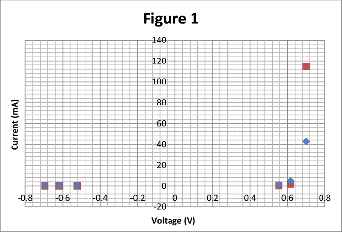
Figure 1: Theoretical points from the Shockley diode equation are in blue. Measured data points are in red. An arbitrary ideality factor of n = 1.5 was used in the Shockley diode equation. The discrepancy between measured and theoretical values might disappear if the true ideality factor of the diode was known.
Wniosek i Podsumowanie
This lab explored the properties of semiconductors and a p-n junction in the form of a semiconductor diode. A diode is a circuit component composed of one p-n junction. The characteristic curve of the diode was measured, and the diode was observed to conduct an electrical current in only one direction. An LED contains a special type of p-n junction that emits light in addition to conducting unidirectionally.
Semiconductors are used extensively in the electronics industry. Semiconductor diodes contain only a single p-n junction, while transistors are made from n-p-n and p-n-p junctions; that is, two p-n junctions directly next to each other. Semiconductor transistors are the basis of nearly all modern electronics. They can be used to construct logic gates, which are circuits that can perform basic Boolean logical operations such as AND, OR, NOT, and NAND. These logical operations can be combined to perform more complex operations such as addition and multiplication, and can even be used to build computer processors and memory. LEDs made from semiconductors are more energy-efficient light sources than traditional incandescent bulbs.
Tagi
Przejdź do...
Filmy z tej kolekcji:

Now Playing
Semiconductors
Physics II
29.8K Wyświetleń

Electric Fields
Physics II
77.4K Wyświetleń

Electric Potential
Physics II
104.4K Wyświetleń

Magnetic Fields
Physics II
33.4K Wyświetleń

Electric Charge in a Magnetic Field
Physics II
33.7K Wyświetleń

Investigation Ohm's Law for Ohmic and Nonohmic Conductors
Physics II
26.2K Wyświetleń

Series and Parallel Resistors
Physics II
33.1K Wyświetleń

Capacitance
Physics II
43.7K Wyświetleń

Inductance
Physics II
21.5K Wyświetleń

RC/RL/LC Circuits
Physics II
142.8K Wyświetleń

Photoelectric Effect
Physics II
32.6K Wyświetleń

Reflection and Refraction
Physics II
35.9K Wyświetleń

Interference and Diffraction
Physics II
90.9K Wyświetleń

Standing Waves
Physics II
49.7K Wyświetleń

Sound Waves and Doppler Shift
Physics II
23.4K Wyświetleń
Copyright © 2025 MyJoVE Corporation. Wszelkie prawa zastrzeżone