Introduction to the Power Pole Board
Overview
Source: Ali Bazzi, Department of Electrical Engineering, University of Connecticut, Storrs, CT.
DC/DC converters are power electronic converters that convert DC voltages and currents from a certain level to another level. Typically, voltage conversion is the main purpose of DC/DC converters and three main types of conversion exist in a single converter: stepping up, stepping down, and stepping up or down. Among the most common step-up converters are boost converters (Refer to this collections video: DC/DC Boost Converter), while among the most-common step-down converters are buck converters. (Refer to this collections video: DC/DC Buck Converter.) Buck-boost converters are also common to perform both step-up and step-down functionalities, and flyback converters can be considered as special types of buck-boost converters where electrical isolation is achieved between the input and output ports. (Refer to this collections video: Flyback Converter.)
DC/DC converter topologies are numerous, and their control, modeling, and operational improvements (e.g. efficiency, reliability, performance, etc.) are areas of continuous interest. The HiRel Power Pole board presented in this experiment provides a very flexible tool to study and analyze the performance of boost, buck, and flyback converter, all on a single board.
The objective of this experiment is to introduce the major components and capabilities of the Power Pole Board from HiRel systems, which is the board being used in three experiments on DC/DC converters.
Principles
The HiRel Power Pole board has five major sub-circuit areas that are labeled in Fig. 1. (Areas labeled in Fig. 1 are approximate.) The first area (red) includes the primary side which has filter capacitors, a current sensor, and connectors labeled "V1" and "COM," which can connect to a DC voltage source or load. Fig. 2 shows a zoom in at the first area with labeled components.
The second area (yellow) includes the secondary side, which has filter capacitors, a current sensor, and connectors labeled "V2" and "COM," which connect to a DC voltage source or the load shown as a planar power resistor. Fig. 3 shows a zoom in at the second area with labeled components. Either the first or second area can be used to connect to a DC voltage source, e.g. DC power supply, while the other connects to a load. Note that when the second area is connected to a source, the load resistor can be unsoldered from the board or left without having impact on the converter's operation as it would be directly fed from the DC voltage source.
The third area (green) is the power-pole area, where two MOSFETs and two diodes are connected. The first "leg" includes an upper MOSFET and a lower diode, while the second "leg" includes an upper diode and a lower MOSFET. The actual components of the upper MOSFET and diode are mounted on the same heat sink in the green rectangle of Fig. 1 on the top left side, while the lower MOSFET and diode are mounted on the same heat sink on the bottom left side in the green rectangle in Fig. 1. A zoom-in view on that area is shown in Fig. 4. The other small green rectangle includes gate drivers that take a low-power switching pulse, e.g. pulse-width-modulated signal, and convert it to the appropriate voltage levels that can turn the MOSFETs on and off.
The fourth area (blue) has four connecting points where a daughter board that includes a magnetic component can be mounted. Two boards are used with this board for the DC/DC converter experiments: the first board is the BB board, shown in Fig. 5, which includes an approximate 100 µH inductor; and the second board is the flyback board, shown in Fig. 6, which includes a flyback coupled inductor or transformer along with its R-C-Diode snubber circuit. The snubber circuit helps provide a path for the stored energy of the primary transformer side in one of the flyback converter's operating modes.
The fifth area includes low-power electronics that generate switching pulses to the MOSFETs, and provide protection to the board including over-current and over-voltage protection. A separate DC power supply is connected to the bottom left of the board, next to switch "S90" which turns on power to all of the low-power circuits so that the high-power side, i.e. areas 1-4, can function properly. The external DC power supply and its connector that plugs in to the Power Pole board are shown in Fig. 7 and 8, respectively.

Figure 1: HiRel Power Pole Board with Five Major Areas Please click here to view a larger version of this figure.
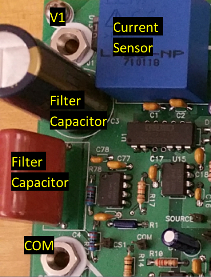
Figure 2: Zoom-in of Area 1.

Figure 3: Zoom-in of Area 2.

Figure 4: Zoom-in of Area 3.

Figure 5: BB Board.

Figure 6: Flyback Board.

Figure 7: External power supply for the low-power electronics.

Figure 8: External power supply connector.
Procedure
This procedure mainly focuses on the ability of the Power Pole board to adjust switching pulses to the upper and lower MOSFETs
1. Setup
- Connect the external DC power supply to the Power Pole board.
- Turn on "S90."
- Observe that the green LED turns ON.
- Check the locations of "S90" and the green LED in Fig. 9.
- Place the second sliding switch in the blue switch array on "Int. PWM. Check the location of the sliding switch array in Fig.10.
- Int. PWM" setting means that the switching pulse (PWM: Pulse width modulation) to either MOSFET is generated on the Power Pole board itself.
- Ext. PWM" means that the switching pulse to either MOSFET is generated by an external source, e.g. function generator or micro-controller.
- Place the first sliding switch in the blue array on "TOP FET." Only one PWM signal is generated on the Power Pole Board, therefore one of the MOSFETs has to be selected as the receiving pulse. Once a MOSFET is selected, that MOSFET should now be able to switch on and off.
- TOP FET "selection means that the upper MOSFET will be receiving the switching pulse.
- BOT FET" selection means that the lower MOSFET will be receiving the switching pulse.
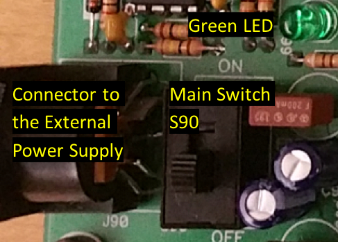
Figure 9. External Power Supply Connector, Main Switch, and LED Indicator

Figure 10. Slider Switch Array
2. Measurements to Monitor the MOSFET Gate Pulses
- Turn on an oscilloscope.
- Connect a regular 10x probe to the oscilloscope's Channel 1.
- Set up the oscilloscope Channel 1 to be in DC coupling to see the PWM offset.
- Set up Channel 1 to be scaled for a 10x probe.
- Set up Measurements on the oscilloscope to measure the frequency and positive duty cycle of the signal to be measured on Channel 1.
- Hook the probe's measuring clip to the "PWM" pin shown in Fig. 10.
- Connect the probe ground to the "GND" pin shown in Fig. 10.
- On the oscilloscope screen, observe a pulse-train which is the PWM signal going to the upper-switch gate driver.
- To ensure that the upper MOSFET is switching, remove the probe's measuring clip and hook it to the "Gate" pin on the top left of the upper MOSFET shown in Fig. 11. You should observe a similar waveform to that you saw when the PWM pin was being probed.
- To ensure that the lower MOSFET is not switching, remove the probe's measuring clip from the upper "Gate" pin and place it on the lower "Gate" pin shown in Fig. 11. You should observe zero voltage.
- Re-place the probe's clip on the "PWM" pin.
- Adjust the duty cycle of the "PWM" signal by changing the potentiometer's knob shown in Fig. 12. Going clockwise increases the duty cycle from zero to 100%, and going counter-clockwise decreases it.
- Adjust the PWM frequency by turning the potentiometer's screw shown in Fig. 13. Use a small screwdriver to adjust the screw's position.
- Observe that the number of pulses displayed on the oscilloscope screen increases or decreases as the potentiometer is adjusted.
- Repeat the above procedure with the BOT FET selection and check to make sure that the lower MOSFET gate is now seeing a switching pulse
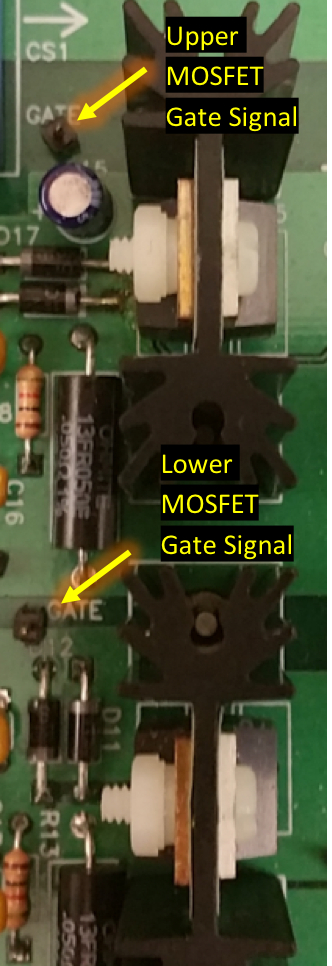
Figure 11: Gate signal pins.

Figure 12: Potentiometer Duty Cycle Adjustment.
Figure 13: Potentiometer for Frequency adjustment
3. Shut down the circuit
- Turn off "S90."
- Disconnect the external DC power supply.
- Disconnect the oscilloscope from both sides.
- Turn off the oscilloscope.
Results
A PWM pulse is expected to be seen on the oscilloscope screen. The duty cycle is a major control variable for DC/DC converter as it adjusts the period during which a MOSFET or any other semiconductor actively-controlled switch is on. All input-output voltage relationships of DC/DC converters rely on the value of this duty ratio, along with some other variable in some converter topologies.
The switching frequency is critical in component selection as the maximum operating frequency of components varies by component type and design. Higher switching frequencies typically yield smaller voltage and current ripples but require larger capacitors and inductors.
Application and Summary
DC/DC converters are very common in DC power supplies used to charge electronics, and to supply power to many other electronic circuits. For example, any motor drive will require some smaller DC power supplies to power its low-power electronics, protection circuits, and high-power gate drives. Computer processors and other peripherals and accessories require very well-regulated DC voltages that are provided by DC power supplies. Renewable energy systems, e.g. solar photovoltaic panels, require DC/DC converters to regulate the DC output voltage of the panels, since solar irradiance and ambient temperature vary causing variation in the solar panel's voltage and current outputs. Many more industrial, transportation, military, and other applications use DC/DC converters instead of linear regulators due to their high efficiency, high performance, and excellent regulation.
Skip to...
Videos from this collection:

Now Playing
Introduction to the Power Pole Board
Electrical Engineering
12.4K Views

Electrical Safety Precautions and Basic Equipment
Electrical Engineering
144.6K Views

Characterization of Magnetic Components
Electrical Engineering
15.0K Views

DC/DC Boost Converter
Electrical Engineering
56.8K Views

DC/DC Buck Converter
Electrical Engineering
21.1K Views

Flyback Converter
Electrical Engineering
13.2K Views

Single Phase Transformers
Electrical Engineering
20.1K Views

Single Phase Rectifiers
Electrical Engineering
23.4K Views

Thyristor Rectifier
Electrical Engineering
17.5K Views

Single Phase Inverter
Electrical Engineering
17.9K Views

DC Motors
Electrical Engineering
23.4K Views

AC Induction Motor Characterization
Electrical Engineering
11.6K Views

VFD-fed AC Induction Machine
Electrical Engineering
6.9K Views

AC Synchronous Machine Synchronization
Electrical Engineering
21.6K Views

AC Synchronous Machine Characterization
Electrical Engineering
14.2K Views
Copyright © 2025 MyJoVE Corporation. All rights reserved